PCB (Printed Circuit Board) packaging engineering is a specialized branch of electrical engineering that focuses on the design, assembly, and integration of printed circuit boards and their enclosures. This field encompasses various aspects, such as thermal management, signal integrity, mechanical stability, and electromagnetic compatibility. PCB packaging is crucial for ensuring optimal performance, reliability, and manufacturability of electronic devices.
In this discipline, engineers apply principles from materials science, mechanical engineering, and electrical engineering to create effective packaging solutions that protect sensitive electronic components, facilitate heat dissipation, and maintain signal integrity. They utilize advanced modeling tools, simulation software, and prototyping techniques to determine the best material combinations and structural designs that meet both performance requirements and cost constraints.
Ultimately, PCB packaging engineering is integral to the development of modern electronic products, from consumer electronics to medical devices and aerospace applications, ensuring they operate reliably under various conditions and have a long service life.
Understanding PCB Quote Packaging Engineering
Printed Circuit Boards (PCBs) serve as the backbone of modern electronics, facilitating the electrically conductive paths for components to function as intended. Within this sphere, PCB quote packaging engineering transcends conventional electrical engineering, incorporating multidisciplinary strategies aimed at optimizing a product’s overall efficacy. To fully grasp this engineering type, it is imperative to explore its components, processes, and relevance in various industries.
1. What is PCB Quote Packaging Engineering?
PCB quote packaging engineering is a subset of electrical and materials engineering dedicated to designing, assembling, and integrating an electronic circuit’s layout and housing. This discipline ensures that printed circuit boards fit optimally within their enclosures while protecting intricate electronic components from environmental stressors like moisture, dust, and physical damage. The engineering also significantly addresses heat dissipation and signal integrity, ensuring that electrical signals flow efficiently and without degradation.
2. Key Components of PCB Quote Packaging
2.1 Material Selection
One of the primary focuses of PCB packaging engineering involves selecting suitable materials that can endure specific operational environments. Common materials include:
- FR-4: A glass-reinforced epoxy laminate widely used for PCBs due to its excellent electrical properties.
- Polyimide: Used for flexible PCBs, this polymer withstands high temperatures and offers excellent mechanical strength.
- Metal Core PCBs: Ideal for high-power applications, these PCBs incorporate metal substrates for improved heat dissipation.
2.2 Design Considerations
Engineers need to consider factors like board layout, trace width, and spacing for optimal current flow, which influence PCB performance. Key design elements include:
- Thermal Management: Effective heat dissipation strategies are integral, including the use of heat sinks and thermal vias.
- Signal Integrity: Minimizing electromagnetic interference (EMI) and maintaining the quality of signals is crucial, often done through careful routing and component placement.
- Mechanical Support: Ensuring adequate mechanical support to prevent flexing and cracking during assembly and use.
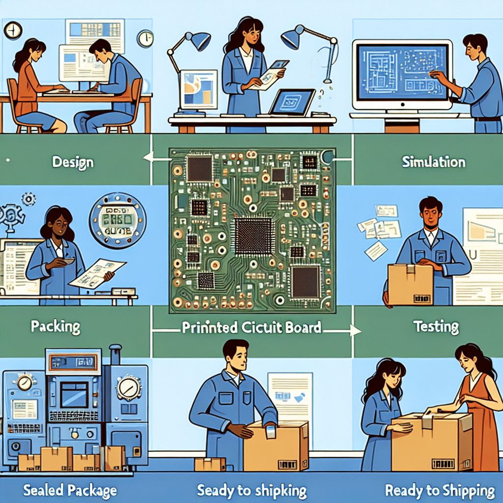
3. The Packaging Process
The PCB packaging process includes several steps that interlink the moment the PCB design is formulated to the completion where it’s ready for market:
- Design: Creation of the PCB schematic followed by a layout using CAD software.
- Prototyping: Initial physical PCB production for testing purposes to assess design feasibility.
- Testing: Rigorous examination for electrical performance, thermal behavior, and reliability under various conditions.
- Production: Mass manufacturing post successful validation of the prototype.
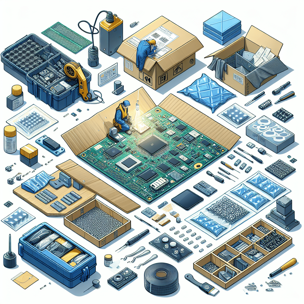
- Post-Production Packaging: Final assembly includes additional protective measures like conformal coatings to guard against moisture.
4. Importance of PCB Packaging Engineering
The significance of PCB packaging engineering cannot be overstated, particularly in an era where miniaturization and multi-functionality are paramount. Well-designed PCB packaging enhances:
- Reliability: Proper packaging mitigates risks of component failure, ensuring performance consistency.
- Cost Efficiency: Optimized designs reduce material waste and facilitate lower production costs.
- Market Competitiveness: High-quality, robust designs meet increasing consumer demands for durability and performance in various electronics.
5. Applications of PCB Packaging Engineering
PCB packaging engineering finds relevance across multiple sectors:
5.1 Consumer Electronics
From smartphones to televisions, reliable PCB designs ensure robust functionality and long-term durability, catering to consumer expectations.
5.2 Automotive Industry
Modern vehicles possess numerous electronic components that require effective packaging engineering to withstand extreme conditions while maintaining performance.
5.3 Medical Devices
Precision in PCB packaging is crucial in medical devices directly impacting patient health; thus, adherence to stringent regulations and standards is mandatory.
5.4 Aerospace and Defense
In sectors that prioritize reliability and performance under adverse conditions, PCB packaging engineering is vital for ensuring operational integrity.
6. Challenges in PCB Packaging Engineering
Professionals encounter various challenges:
- Size Constraints: Miniaturization demands innovative designs that maintain functionality without compromising performance.
- Cost vs. Quality: Balancing cost-effective manufacturing while ensuring high-quality components can challenge profitability.
- Rapid Technological Advancements: Staying abreast with advancements in materials and techniques is fundamental for continual improvement.
7. Future Trends in PCB Packaging Engineering
To remain competitive, several trends will shape PCB packaging engineering:
- Smart Systems: Integration of IoT within PCBs facilitates connectivity and monitoring, increasing complexity.
- Advanced Materials: The exploration of new materials such as biodegradable substrates and advanced composites for sustainability.
- 3D Packaging: Vertical stacking of components and PCB layers to optimize space while maintaining thermal and electrical performance.
FAQs
What qualifications do PCB packaging engineers have?
PCB packaging engineers typically possess degrees in electrical engineering, materials science, or a related field and often undergo specialized training in PCB design and manufacturing.
Are PCB packaging engineers involved in the manufacturing process?
Yes, PCB packaging engineers collaborate closely with manufacturing teams to ensure that designs are feasible and can be produced efficiently while meeting quality standards.
What industries rely on PCB packaging engineering?
PCBs are critical in various industries, including consumer electronics, automotive, medical devices, and aerospace sectors, making PCB packaging engineering essential for safeguarding performance and reliability.
How can I improve my PCB designs?
Improve PCB designs by using simulation tools for testing layouts, optimizing material choices for heat dissipation, and adhering to industry standards for best practices.