Introduction
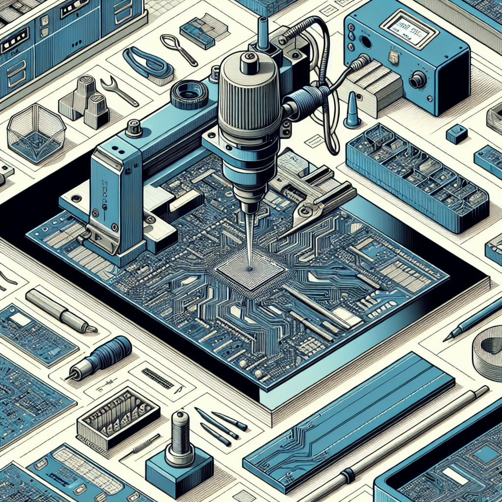
A beveler in PCB (Printed Circuit Board) manufacturing is a specialized tool or process used to create angled edges on the board’s surfaces. This technique improves the solderability and aesthetic appeal of PCBs, especially in high-density applications. By beveled edges, manufacturers can ensure better connections, reduced stress concentrations, and improved electrical performance. The beveling process helps alleviate issues related to solder mask registration and can reduce the risk of components shorting during assembly. In the context of modern electronics, where precision is paramount, the use of a beveler in PCB fabrication has become increasingly essential for enhancing both reliability and manufacturability.
Understanding Beveling in PCB Manufacturing
What is Beveling?
Beveling is a machining process that cuts an angle into the edge of an object, typically to facilitate assembly or enhance functionality. When it comes to PCBs, beveling can feature different angles, commonly ranging from 30 to 45 degrees. This process is often employed to prepare PCB edges for soldering, providing a larger surface area for solder joint creation. Additionally, beveling minimizes the risk of damage to the PCB during handling and installation.
Importance of Beveling in PCBs
The importance of beveling in PCB manufacturing can be attributed to several factors:
- Enhanced Solderability: Beveled edges allow solder to flow more easily, creating stronger and more reliable joints.
- Reduced Mechanical Stress: Sharp edges can create stress concentrations; beveling distributes these stresses more evenly across the PCB.
- Aesthetic Appeal: Beveled edges offer a more professional appearance, desired in many modern electronic devices.
- Improved Compatibility with Components: Bevels help prevent difficulties when inserting components, particularly in crowded layouts.
Types of Beveling Techniques
Manual vs. Automated Beveling
Beveling can be conducted manually or through automated processes. Manual beveling involves the use of hand tools, while automated beveling utilizes CNC machines or specialized beveling machines. Automated systems typically yield higher precision and consistency, making them more suitable for high-volume production.
Common Beveling Methods
- Router Beveling: This method uses a rotating tool to create angled edges along the PCB paths.
- Laser Beveling: A highly precise method that uses a focused laser beam to melt and shape the PCB edges.
- Water Jet Beveling: The use of high-pressure water streams to cut and bevel PCB edges without damaging the material.
Key Considerations in Beveling PCBs
Material Type
The choice of beveling technique may vary based on the type of substrate material. FR-4, a widely used material in PCB fabrication, has different milling and cutting characteristics compared to other materials like polyimide or ceramic substrates. Understanding the material’s properties is critical in choosing the correct beveling process.
Precision Requirements
In applications where precision is paramount, such as aerospace or medical devices, the beveling process must adhere to stringent tolerances. Automated techniques like CNC routing offer consistent results and can be programmed to achieve exact specifications.
Cost Considerations
The cost of beveling varies based on the method chosen. Manual processes typically have lower initial costs but may incur higher labor costs over time. Automated solutions, while initially expensive, are cost-effective in high-volume scenarios due to their speed and efficiency.
Industry Standards and Best Practices
Adhering to industry standards is crucial for ensuring that PCBs meet necessary performance requirements. Governing bodies such as IPC (Institute for Printed Circuits) establish guidelines regarding beveling processes to maintain quality and reliability.
FAQs About Bevelers in PCB
What are the benefits of beveling PCBs?
The benefits include enhanced solderability, reduced mechanical stress, improved aesthetics, and better compatibility with components.
What materials can be beveled?
Commonly beveled materials include FR-4, polyimide, and ceramic substrates, each requiring tailored beveling techniques.
How does beveling affect PCB reliability?
Beveling improves PCB reliability by reducing sharp edges that can lead to damage and ensuring effective solder joint formation.
Is automated beveling more efficient than manual beveling?
Yes, automated beveling typically offers greater efficiency and consistency, particularly in high-volume production contexts.
What are the common bevel angles used in PCB manufacturing?
Common bevel angles range from 30 to 45 degrees, depending on design specifications and soldering requirements.
Conclusion
Understanding the functionality and advantages of beveling in PCB fabrication is essential for anyone involved in electronic manufacturing. By utilizing advanced techniques and adhering to industry standards, manufacturers can significantly enhance the quality and performance of their PCBs. As technology evolves, the role of beveling will only continue to grow, making it a critical aspect of PCB design and production.